


 Nolan’s Notes: Moving Forward With Confidence
 The Knowledge Base: Beyond the Badge—Why Membership Matters More Than Ever
 Smart Automation: AI—Revolutionizing Inspection in Electronics Manufacturing


Transition Automation Updates Innovative Paste Retainers
September 27, 2023 | Transition Automation, Inc.Estimated reading time: Less than a minute
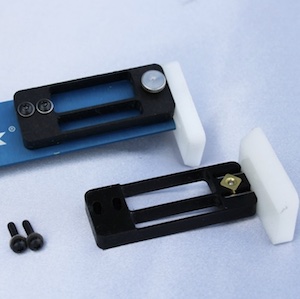
Transition Automation, Inc. has improved the unique Paste Retainer System that is included in the company’s line of squeegee holder systems. The Soft-Touch™ Paste retainers now have a dual pin locking that better secures the white dam portion. Additionally, the attachment screws have been upgraded to Alloy Steel compared to the previous galvanized steel. The spring element is made thicker, giving the design more impact resistance. The total part count was reduced by 8 pcs per set. The white dam may be adjusted in or out based on the position of the squeegee blade, and the entire assembly can be adjusted up or down to push against the stencil or to ride above it slightly. This new design affords faster maintenance for cleaning and easer use.
The Soft-Touch Paste retainer system is an integral part of Transition’s advanced squeegee holder system. These devices help keep the solder paste inside the print area.
Share on:


Suggested Items
BEST Inc. Introduces StikNPeel Rework Stencil for Fast, Simple and Reliable Solder Paste Printing
06/02/2025 | BEST Inc.BEST Inc., a leader in electronic component rework services, training, and products is pleased to introduce StikNPeel™ rework stencils. This innovative product is designed for printing solder paste for placement of gull wing devices such as quad flat packs (QFPs) or bottom terminated components.
Indium to Feature Materials Solutions for Semiconductor Packaging and Assembly at ECTC
05/22/2025 | Indium CorporationIndium Corporation®, an industry leader in innovative materials solutions for semiconductor packaging and assembly, will feature its lineup of high-reliability products at the Electronics Component and Technology Conference (ECTC), taking place May 27-30 in Dallas, Texas.
Indium’s Karthik Vijay to Present on Dual Alloy Solder Paste Systems at SMTA’s Electronics in Harsh Environments Conference
05/06/2025 | Indium CorporationIndium Corporation Technical Manager, Europe, Africa, and the Middle East Karthik Vijay will deliver a technical presentation on dual alloy solder paste systems at SMTA’s Electronics in Harsh Environments Conference, May 20-22 in Amsterdam, Netherlands.
Libra Industries Boosts SMT and Electronics Manufacturing Capabilities in Dallas, Texas
05/06/2025 | Libra IndustriesLibra Industries is excited to announce the latest upgrades to its surface mount technology (SMT) capabilities at its Dallas, Texas facility.
Happy’s Tech Talk #38: Novel Metallization for UHDI
05/07/2025 | Happy Holden -- Column: Happy’s Tech TalkI have been involved in high-density electronics substrates since 1970 when I joined Hewlett-Packard’s RF semiconductor group after college. Figure 1 shows the difference between trace/space lithography for substrates and silicon starting in 1970. My projects involved sapphire circuits for RF devices, but the figure displays the state of PCBs and integrated CMOS circuits and their packaging, not discreet RF devices. Even then, semiconductors were 50X higher density.